About some Class D amplifier (TI TPA3116D2) boards.

I bought a bunch of these boards a few years ago [Photo 1], and over the past few months (a definate Covid project) I built up a “desktop amp” to make use of a couple of them. (an eBay search [March 2021] did not turn up any modules that looked the same: there are a LOT of boards for sale using this chip!). The amplifier also used several items that I had on hand: a scavenged motorized volume control; some surplus aerospace-quality latching relays and one of my own L'ilBoard Arduino pro mini clones to control the relays and the pot. The performance of the result did not impress me, so I started looking at the design. {I have, in the past, designed boards for customers that use the very same chip so I know a bit about how to care for and feed these ubiquitous ICs.}
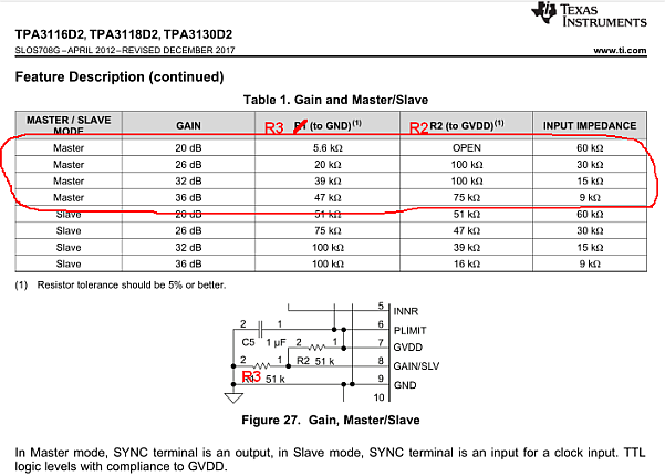
The first thing I noticed is that the two resistors which are used to set the gain and clock mode do not correspond to the suggested values in the datasheet. These connect to the GAIN/SLV pin, and there are 8 allowable/suggested value pairs for these as shown in Table 1 of the data sheet. These boards are set up with the resistor to ground as 100 kΩ: that matches up with two of the lines in that Table, but the value of the resistor to the supply is neither 39 kΩ nor 16 kΩ: instead it is 47 kΩ. Regardless of the exact value of gain (either 32 dB or 36 dB) which is obtained by this pair of resistors it is clear that the amps are set up as slave devices. That means that the SYNC pin (pin 16) should be driven by a clock, but wait! That pin is grounded on these boards! As far as I can tell this is not a valid way to operate them!
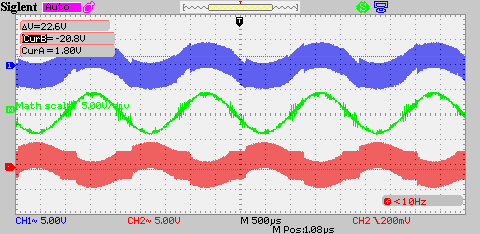
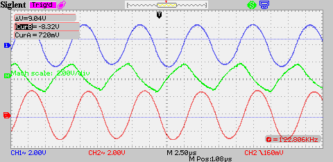
A further clue is what is happening at the outputs: [Images 1 and 2, below] shows a switching frequency of about 120 kHz. This is NOT right: the minimum switching frequency is 400 kHz. The frequency is set by how pins AM0, AM1 and AM2 are wired (see the AC Electrical Characteristics table, section 6.6, page 7 of the data sheet). These pins are all grounded so the operating frequency should be between 376 kHz and 424 kHz.
This low frequency would explain a lot:
- I found that one of my boards was operating at near 124 kHz and the other at about 121 kHz: I suspected that the beat frequency of these two numbers was getting into the audio.
- The waveforms at the outputs have way too much of the switching signal on them [image 1]. This no doubt due to the lower frequency: the ouput filters conform to TI's design but they are meant to filter signals at least 3 times higher.
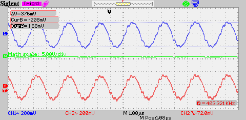
So, I suspected that this extremely low switching frequency was a result of being in slave mode with no clock provided. To confirm this I set up one of the boards to operate as a 32 dB gain master. This made a huge difference at the outputs: [image 3] shows the results with the same input conditions as [image 2], but note that the scope's vertical scales are 10x more sensitive. What was more than 5 Vp-p at 120 kHz is now less than 400 mVp-p at 403 kHz. This is a reduction of about 22 dB. More impoortantly the difference signal is reduced from about 3.2 Vp-p to much better than 0.1 V, or at least -30 dB.
If you have some of these boards.
Modifications suggested below require that you are able to remove and replace size 0603 surface mount resistors AND that you can lift pin 16 from the pad it is connected to and, depending on whether you need to make a board the master clock source and one or more other boards to be slaves, then some very delicate solder iron work is needed. If you think you can perform the first two tasks but not the third, then it might be OK to run a system with multiple masters.
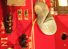
If you have just one, the minimum modification you should make is to lift pin 16 (see below) and change the on-board resistors R3 and R2 to match one of the lines within the circled section of Figure 1. These resistors are just in from the input header. The heat sink is best removed to allow soldering iron access even though these parts are not under it.
Lifting pin 16.
It is quite convenient that pin 16 is a corner pin since this makes it relatively easy to lift. I used a sharp tipped knife to gently pry the pin up while heating the solder. A small dental probe or pick should work too. Cleaning off the pad using some fine solder wick then slipping over some sleeving ensured that the pin does not re-connect with the pad when the heat sink is bolted on.
If you have more than one of these in the same system, then it is best to modify one as a master and the rest to be slaves at the same gain setting. This entails adding a wire to each chip's pin 16 after the pins are lifted from their ground pad. [Photo 2] shows a board modified as master. (You probably can't see but R2 is 100 kΩ and R3 is 39 kΩ.) The yellow AWG 30 wire was soldered mid-air to the lifted pin then a bit of sleeving was used to ensure isolation. The tacky stuff was added as extra assurance.
Results.
Previously, when trying to track down a just audible speaker “whistle” it was quite difficult to see the tree for the forest of ~120 kHz signals. These were on the power supply, the grounds and basically everywhere!
Also, previously I had noticed that the output filter inductors were warm even with no audio input. This is gone now: it was likely due to the roughly 3.2 Vp-p signal as seen in Image 2.
One interesting observation is that the frequency put out on the SYNC pin is ONE QUARTER of the switching frequency. There seems to be no mention of this in the data sheet, nor is a 4x phase lock loop shown in the block diagram which would be necessary when operating as a slave! I checked the latest revision online too (it is at Rev G, December 2017). The existence of a PLL would probably explain why the chips still worked with no SYNC input: generally a PLL will have an oscillator which will still run with no input to sync to, at a low frequency.