A guide to setting up the LM2907 (& LM2917) frequency to Voltage converters.
I had
occasion to use an LM2907 to convert a digital pulse train to a voltage. I found the datasheet a
poor match for my particular brain, so I decided to dig into how the part works. There are no
wavefoms to speak of in the
data sheet  (just Figures 16 and 17 on page 15 which show a step response scenario and a particular output
voltage ripple condition, respectively). Also, there are no specifications on the maximum
frequency range that can be expected, nor the minimum power supply operational voltage
range. I did note that Digi-Key has a figure of 10 kHz for the max. frequency on their page
for the device, but that is nowhere to be seen in the data sheet, and I will show, it is not the
real limitation.
(just Figures 16 and 17 on page 15 which show a step response scenario and a particular output
voltage ripple condition, respectively). Also, there are no specifications on the maximum
frequency range that can be expected, nor the minimum power supply operational voltage
range. I did note that Digi-Key has a figure of 10 kHz for the max. frequency on their page
for the device, but that is nowhere to be seen in the data sheet, and I will show, it is not the
real limitation.
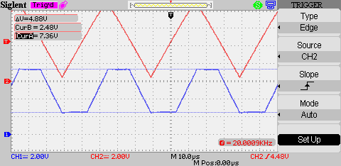
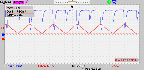
There are two capacitors and one resistor which set up the f to V function. The first cap hangs off of pin 2 to ground and is designated C1 in the data sheet (—or not: some diagrams omit the designations—sloppy!). It integrates a fixed current which is either positive or negative. Two voltage thresholds determine when the current is shut off, and the incoming edges of the signal determine when they turn on: the capacitor charges when the signal rises past a threshold, and it discharges when the signal falls below a lower threshold. [Image 1] shows this, and [Image 2] shows the hysteresis due to the two thresholds.
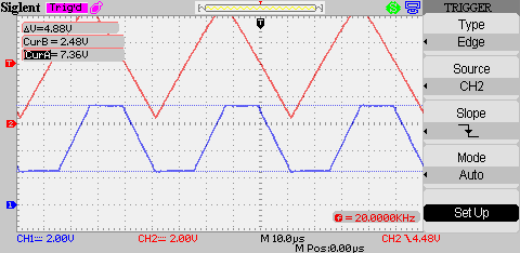
The specified minimum value for C1 is 500 pF. That value and the currents that charge and discharge it will determine the maximum operating frequency. First, let us constrain the input to be a fast rising and falling square wave so that the input hysteresis does not affect the mark/space ratio of the capacitor's waveform. The currents, both charge and discharge, have a nominal 180 µA value, however the data sheet's spec (section 7.5, the “I2, I3” line) is 140 to 240 µA, nominal 180 µA. To determine the maximum frequency for “all” parts, one would have to use the higher value. The voltage swing on the same capacitor is a function of the supply voltage because the thresholds are, and is defined in section 7.5, note 2 as: “V OH = 0.75 × VCC-1 VBE and V OL = 0.25 × V CC-1 V BE, therefore VOH-VOL = VCC/2”. Now, I don't see these voltages to be exactly as advertised. I ran the chip at various supply voltages and measured the high and low voltages of the pin 2 waveform, giving the plot of [Figure 1]:
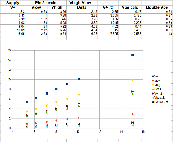
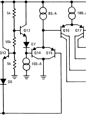
In an attempt to figure out what these two levels actually are, the spreadsheet shown in [Figure 1] calculates the stated value (V+/2) to compare against the difference of my measured levels. It is clear that there is at least a rough linear reduction in the peak to peak magnitude of the waveform vs. the stated value of half supply. [Figure 2] captures the portion of the circuit that generates the thresholds. If the schematic is to be taken as literal (one can never be sure of that) then it looks more like the thresholds are 0.75 × and 0.25 × V CC; each minus a diode drop, not a VBE. (The VBEs of Q12 and Q15 would cancel as would those of Q13 and Q14 respectively).
Not shown in [Figure 1] I also had the spreadsheet calculate the ratio of the peak-to-peak difference of the waveform to half VCC. This came to very close to 0.46 for the entire supply range I tried. That is about 8% down from the data sheet's stated value. Whether my few parts are exceptions I cannot know, but since it is proprtional to the supply voltage, I'd imagine that it is consistent with a resistor ratio error.
Now, the maximum frequency.
So the maximum frequency is determined by the longest possible time that a minimum value for C1 takes to ramp up and down again where the waveform does not show a flat top or bottom. That is 2×Δt where Δt=ΔV×C1/I2 and C1 is at the worst case maximum value and I2 is at the lowest possible value. Using a 560 pF, 10% capacitor (a good practical value since 560-10% is still over the minimum of 500 at 504 pF) and the minimum specified current of 140 µA, I get from about 45 kHz at VCC= 5 V to about 16.3 kHz at 15 V. If the maximum current happened to be produced by the part being used, and the capacitor was trimmed to exactly 500 pF then it could operate at up to more than 120 kHz at a 5 V supply, but that cannot be counted on. Also, it is likely best to stay safe and use the 50% VCC value since that lowers the maximum frequency by the 8% found above.
What is the supply range?
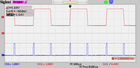
As stated in the introduction, there is no recommended supply voltage range. All that is known is that 28 V is the extreme value. I decided to try to get the chip to run at as low a supply as it would still function. I got down to 3.5 V (anything under exhibited severe jitter on the waveform) and by carefully adjusting the input I got it to run at more than 100 kHz, [Image 3].
My application.
So far I have not said anything about my application. I am converting the 0 to 25 kHz frequency
from a Mach 3-driven parallel port card to a 0 to 10 V signal to control a Variable Frequency
Drive (VFD) in a CNC system. In essence I'm partially replicating a “C6R6” board. It is
not clear from its manual whether they are running their LM2907 at 12 V (the board does use this voltage but there
might be another regulator) or a lower voltage, nor are any other key circuit details available.
Based on my calculations above, I suspect they are running it at something like 5 V since
operation would not be assured to 25 kHz at 12 V.
I decided, however to run it at 12 V, and to divide the incoming frequency by 2. I used a CD4093 (quad NAND gate with Schmitt trigger inputs) to square up the edges following an opto-isolator. The slew rate of the edges are important for the CD4013 used to divide by 2. This approach ensures that the duty cycle of the LM2907's input is an “exact” 50% which helps maintain the maximum frequency range. That could matter since 12.5 kHz is fairly close to the calculated 18.9 kHz worst case maximum running at 12 V.
The rest of the chip.
I have not yet covered the functionality which produces a voltage proportional to the input frequency. What happens is that both the rising and falling edges of C1's waveform are converted to positive-going current pulses on pin 3 [Image 4]. The magnitude of the current is the same as the pulses in and out of pin 2: I3 == |I2| since I2 changes direction every half cycle.
The conditions behind [Image 4] do not yet represent the input frequency as a voltage, however all that is needed is a largish capacitor to average the pulses. Since the pulses are driven by a current source they are inherently easy to average. The top level voltage seen in [Image 4] represents the maximum output voltage. It will become the full scale output of the device if/when the pulses merge together at the condition when pin 2 shows a triangle waveform with no flats. So to get, say a 10 V full scale level, then this peak value must also be 10 V.
A suggested design approach.
The data sheet's Equation 2 and also Equation 5 are based on the ΔV being half the supply, so if the ΔV is different, as I found, the reality will not be so clean. So my procedure, below, is based on reality and worst case values.
- Select C1. Ideally pick this component such that pin 2's waveform would peak at both limits assuming the minimum I2 value, 140 µA at your desired maximum input frequency. The limits are, of course determined by the supply. In other words a triangle wave would be produced. If your duty cycle is not near 50%, then you will likely have to use a smaller capacitor to ensure that neither peak of the waveform moves away from the 25%/75% levels. Use C1= I2-min×Δt/ΔV where Δt is half of the period of the desired maximum frequency and ΔV is the peak-to-peak voltage on pin 2 as discussed above. Your peak-to-peak value may or may not be closer to the value that I found, or the 1/2 V cc designer's intention may hold more accurately for your IC. Pick the next lowest standard value, and as always keep the part's tolerance in mind. Also keep in mind the 500 pF minimum. If this cannot be met then your two choices are to lower the chip's power rail or divide down the input frequency digitally.
- Select R1. This sets the maximum output voltage when the output pulses have all merged into a continuous level. That only happens at the maximum frequency if the chip being used is running at the low current value. But, and this is a key point, as long as the I2 and I3 values track then the output V to input f correspondence will be maintained. Algebraically this can be shown because I3-min×R1 will equal I3-max ×R1×(I2-min/I2-max) when I2==I3. What will be different between a chip with lowest I3 vs. one with the highest I3 is that the later will accept a larger input frequency and, assuming no voltage limit is reached, it will output a higher voltage.
- Select C2. The main requirements here are response time traded off for ripple. My application, setting motor speed, does not need quick response. A small value capacitor here of 0.01 µF results in 280 mVp-p ripple at 1 kHz, down to about 12 mVp-p at 30 kHz. A 1 µF tantalum reduces the ripple at the low frequency range substantially, but not at the high end, likely due to its ESR.