Who is MalcoTech anyway?
Makerspace Nanaimo received 9 power supplies all of the same construction from Vancouver Island University [Photo 1]. At first it was not obvious that they were actually manufactured at the institution, but their lack of a manufacturer's nameplate and the name of their apparent manufacturer, "MalcoTech" told the story: not too many years ago VIU was Malaspina College!
As soon as I tried one it was apparent that it did not supply much current: perhaps a clue to why they were being disposed of? Also, some of them could not reach the full 25 V full scale output.
The supplies are built on an aluminum chassis which is contained within a 8" by 8" by 4.5" deep steel cabinet. The front panels (hover over Photo 1 to see an individual supply close up) are dominated by two analog meters, one reads voltage on a 25 V scale and one indicates current on a 250 mA scale. Below the voltmeter are coarse and fine voltage adjustment potentiometers, and below the current scale is a 2-position switch with "X1" and "X10" labels, which is above a current limit-setting pot. Apparently the switch is meant to switch both the current limit and meter scale between 250 mA and 2.5 A.
Circuit Sleuthing
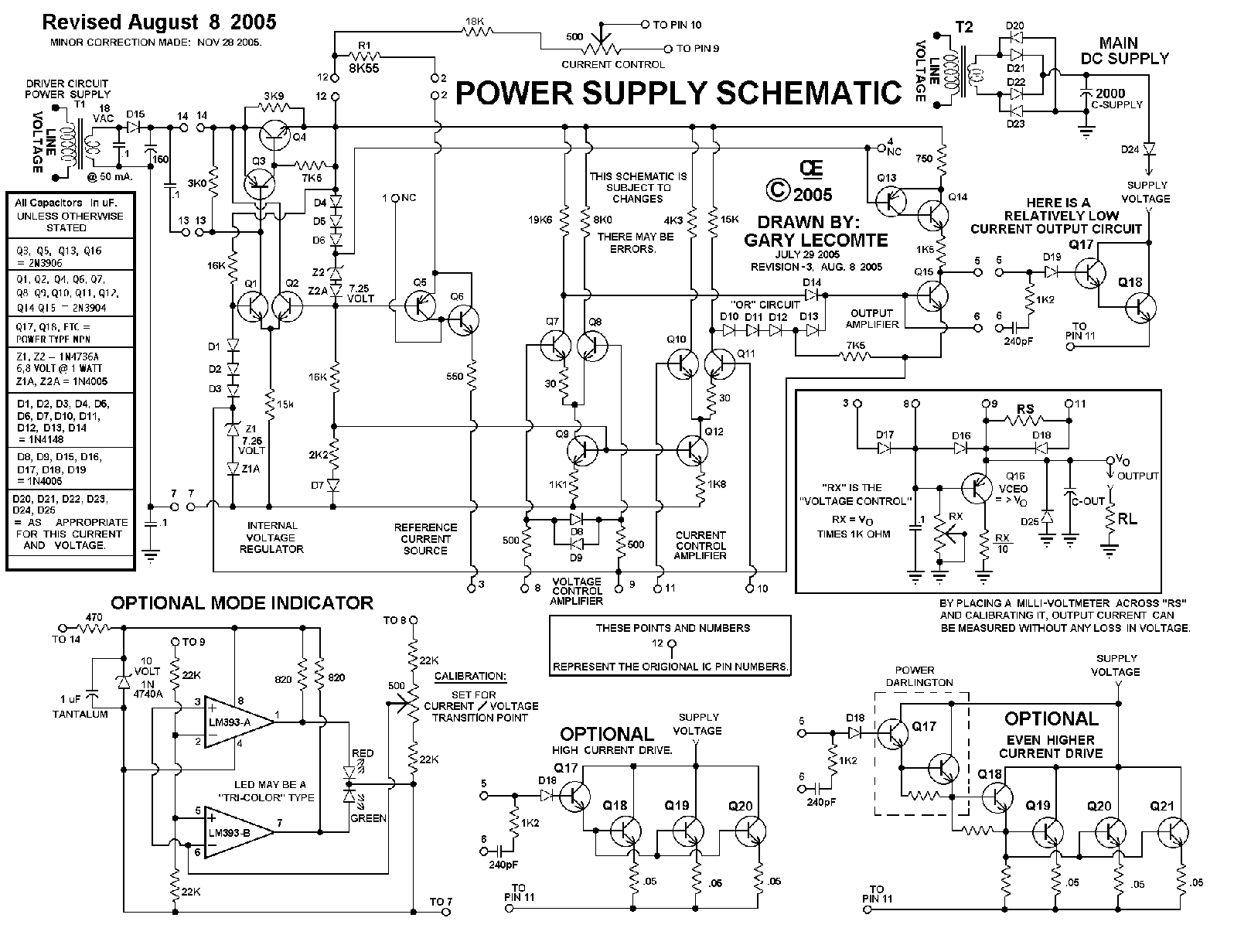
Once I opened a supply up, though, it seemed odd that it did not supply much current: the main transformer is a 25 Vac 3 A unit (Hammond 167M25, which can still be bought, for about $55 Cdn), and the series pass transistor is a venerable 2N3055 NPN power device which is also still available and is up to the job. The control circuitry is built on a plug-in PCB and is designed around a Motorola MC1466 IC, a chip which is no longer available [click here to go to a sidebar, below]. Most, but not all of the PCBs have had a stamp applied showing a 1990 date. This is many years newer than the date codes on the ICs which are in the 1969 to 1970 range! Note that the College was officially opened in the fall of 1969. 
Figure 1 shows the original wiring. The current sense resistors are either 1.5 Ohm if the current limit switch is at the "X1" position or 0.33 Ω in parallel with 0.27 Ω and the original 1.5 Ω which computes as 0.135 Ω when at the "X10" position. The IC works by limiting the output voltage when the voltage across the sense resistor reaches 0.25 V, so in the "X1" position that should be 0.25/1.5 = 167 mA and the "X10" should be limiting at 0.25/0.135 = 1.85 A. As you'll see these are theoretical calculations only.
No matter where they are, ohms are ohms!
However a serious design error was made. The designers failed to understand that all connectors have contact resistance, that the magnitude of this resistance is not small compared to the desired parallel resistances they needed and that the resistance can vary with many factors, especially time. The PCB "fingers" used here, which are simply copper tracks with no plating which plug into apparently gold plated sockets are especially poor in this regard. The switch contacts which bring in the lower resistance are also subject to this reality. So it turns out that when the current range switch is in the "X10" position the lower resistance is in series with three unknown and variable resistances. The lower limit setting resistor, the 1.5 Ω part, is in series with two of these as well.
A design change, to remove the range switching and to solder the current sense resistor directly in the current path, proved to be remarkably useful. I soldered a 0.1 Ω resistor directly to the chassis-mounted PCB socket in one unit at the appropriate pins. Immediately the supply could deliver 2.5 A instead of a random limit, typically less than 1 A. In another supply which I attempted to modify this way there were complications preventing the easy installation of the part in the chassis so I decided to try putting the lower value at the site of the original 1.5 Ω component on the board even though I knew this might be a bad idea. This proved to be the case: the supply limited at about 1.65 A, meaning that the actual sense resistance is about 0.25/1.65 = 0.151 Ω. This means that JUST A SINGLE PCB FINGER CONNECTION has a resistance in the order of 50 mΩ! I did go to some extra effort to modify this supply properly after all.
I mentioned above that I removed the range switching. The original current meters are 250 mA full scale units. As stated, the switch contacts have a similar resistance problem. The range switch has two poles, one used to switch in the lower current sense resistance in parallel as described above, and the other to switch in a current shunt in parallel with the meter, presumably with the intention of diverting 2.25 A at full scale so that it measued 2.5 A. Do you have a feel for the problem? The resistance of the shunt needs to be low, less than 50 mOhms! The original wiring used a shunt resistance made from a length of #24 bare copper wire, and the lengths of these shunts, unit to unit, were different! Apparently their lengths had been “tuned” to compensate for the switch resistances at time of manufacture!
Sidebar: What lengths people go to to replace the MC1466!
I wrote above that the MC1466 is no longer made. A recent (April 2018) ebay search, however turned up a multitude of these ICs. Looking at the listing photos it appears that there was a run of the chips in Korea in the late 90's. Whether or not these are clones or not I can't tell, though I'd be surprised if clones were produced in actual ceramic packages. Some of the other listings show fuzzy photos of 14 pin DIPs with no apparent branding, and why would I buy such a chip from a UK seller for almost $40 plus $10 shipping when I can order from China for $7, shipping included?
Anyway, back when I started working on these supplies the chips were not to be found but I did find several people who were “rolling their own”:
- Somebody named Eric who calls his site Tube Time built a miniature PCB plug-in replacement!
- And a fellow BC resident (though Hedley is a bit far from Vancouver Island) built his own version (schematic here) but did not try for a DIP-size form factor.
One thing I find interesting about the IC's design is that it uses a constant voltage to provide the reference to control the current, and in reverse, it provides a constant current source to enable control of the voltage. Something nice and “dual” about that!
So I manufactured new shunts, using a similar wire (but a magnet wire with a proper lacquer type insulation) and installed these directly on the meter terminals. The meter cannot indicate low currents as well as before but it does accurately read the full range which the power supply can now deliver. Of course I also had to change the scales to read 2.5 A full scale instead of the paltry 1/4 A.
Maximum voltage limitation.
The limitation on the highest output voltage was easily traced to the value of “R1” (as designated in the IC's data sheet). This resistor sets a constant current which is conducted through the voltage setting pots. The output voltage will simply be this current multiplied by the resistance that the pots are set to. So a 25 V output using a 20 kΩ coarse setting pot and a 2 kΩ fine setting pot would need a 25/22000 = 1.14 mA current. The value used on several of the boards was a simple 10 kΩ 5% part. Using the data sheet's formula this would only provide a current of 8.55/10 = 0.855 mA, allowing only 18.8 V at the output when the control pots are at maximum. This value is almost exactly what I saw. The fix is easy, just put the proper resistor on the board instead of the 10 kΩ.
Watch your fingers!
Something to watch out for is that the 2N3055 power transistor can dissipate a fair bit of power now. At a nominal internal raw rail voltage of 35 V, and if the supply is driving a short circuit with the full 2.5 A (the worst case), then that is 87.5 W. Given the heat sink and assuming it is reasonably well connected (thermally) to it, that should be within the capabilities of the part, however it might get too hot to touch safely. From the data sheet, the part is allowed to be hotter than about 65C at this level of internal power dissipation. I have not tested this aspect (yet). It would be so much better to be able to lower the internal supply voltage under low output voltage conditions. This could possibly be done if the center tap winding of the power transformer's secondary were made available, and a relay employed to select between full and half voltages. (This is a pretty standard technique in high power, wide voltage range linear supplies.) In the one unit I have taken completely apart the center tap's wire had been cut off inside the power transformer's case, but it could likely be restored by splicing a new wire on.
For Makerspace Nanaimo members, there are now 3 units fully converted and with new 2.5 A current meter scales. One sure way to tell at a glance if a supply is one of these is that the paper I used for the new scale is so much whiter than the background on the voltage scale. As well I included the Makerspace Nanaimo logo on the paper.
The future
Some of the remaining supplies may be treated differently. One contemplated option is to remake them entirely, keeping little more than the power transformer, the bridge rectifier and the large “computer grade” electrolytic filter capacitor (which is actually over specified by at least a factor of 3 for a 2.5 A draw at 25 V output). A modern possibly (isolated) USB-interfaced, Arduino controlled sounds like a great project. Now to get designing...