Board Views.
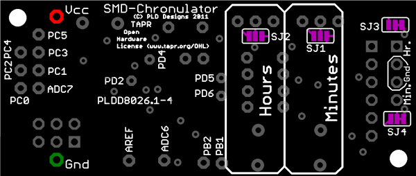
The first two views of the board here highlight the solder-blob jumpers. You can easily see which ones have pre-jumpered sections. The power and ground connections are colour-coded as well. The third view is of the area around the timing crystal.
Top View.
There's just one jumper on the top: if the track is open then reduced power consumption will result since the software disables the serial port when the port input controlled by this line (PC1) is not grounded.

Bottom View.
There are four solder jumpers on the bottom. SJ3 and SJ4 have shorting tracks laid down at PCB
manufacture: these would be opened only if the current sources are not wanted, either to run
different off-board meter drive circuits or when using the board in the Arduino compatible mode.
The two associated with the trim-pots must have a solder blob jumper connecting the center pad to
one of the outer two to allow for proper adjustment of the current sources. See
the set-up page  to determine which side to jump.

Crystals and capacitors.
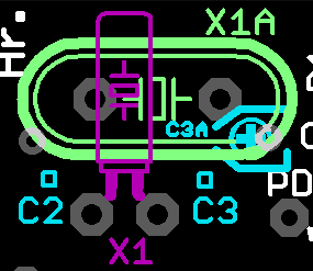
Here's a zoomed in view of the crystal area, both as a graphic and a real photo. In the graphic, I've colour coded the outlines for the “normal” 32 kHz watch crystal, X1, in this colour, and the alternative HC-49 or HC-49S, X1A in this green. The crystal-loading capacitors are highlighted in this colour, where C2 and C3 are 0603-size parts which are normally 18 pF.
C3A is an optional trim cap, and is mostly intended to be used when X1 is installed, though it
should also be able to be installed with X1A if leads are properly dressed, or the crystal is
mounted on the bottom. In the photo you can see how small the pads are for the trimmer. In fact
the pads represent a smaller size than I had intended: the consequence is that the parts that will
fit there cost almost as much as the processor! See the BoM  for a suggested component at C3A.


